6 min read
Three weeks ago, I wrote that Credo’s preannouncement of $404–$408 million in Q3 revenue proved the optical thesis. I laid out three questions the earnings call needed to answer: Was the Q4 deceleration sandbagging or structural? Was customer concentration improving? What was the read-through across the optical stack?
Today, Bill Brennan answered all three — and then dropped something that ties directly to the Memory Wars thesis in a way I didn’t see coming.
Credo reported $407.0 million in Q3 revenue — 51.9% sequential, 201.5% YoY. GAAP gross margin: 68.5%, well above the 63.8%–65.8% guide. Non-GAAP operating margin: 49.6%. EPS of $1.07 vs. Street at ~$0.94. Cash: ~$1.3 billion, up from $813M last quarter.
Q4 guide: $425–$435 million, gross margins stepping back to 64–66%. Not a demand cliff — a mix shift.
In my preannouncement piece, I flagged the concentration risk: “Their largest customer was 86% of Q2 revenue.” The Q&A revealed the new breakdown: largest customer at 39%, second at 32%, third at 17% — the first hyperscaler they ramped. All three grew sequentially Q2 to Q3, but in a different order. Concentration is improving fast.
The fifth hyperscaler is now contributing meaningfully. TensorWave named as first ZeroFlap optics production customer. And the line that matters most: Brennan said the industry remains “early in its AEC adoption.” After a $407 million quarter.
Hours before Credo reported, NVIDIA announced $2 billion strategic investments in both Lumentum and Coherent — $4 billion total into photonics, with multibillion-dollar purchase commitments and future capacity rights. Jensen’s framing: optical interconnects are “critical for the continued scaling of AI factories.” Lumentum is building a new U.S. fab. This is the largest photonics investment in NVIDIA’s history — and it landed the same morning as Credo’s Q3 call.
Then Vivek Arya from Bank of America asked Brennan about copper vs. optical. On the very day NVIDIA validated the transition with $4 billion, Brennan’s answer was unequivocal. He referenced NVIDIA directly: “I think they’ve been really outspoken that where you can use copper, you will use copper.” Then laid out why AECs win over laser-based optics: “Reliability. Number one. Power efficiency number two. And ultimately total cost of ownership.” That equation doesn’t change at 200G per lane / 1.6T — though AEC reach tightens slightly from 7m to 5m.
In my preannouncement piece: “The lazy narrative is ‘copper-to-optical transition.’ The real story is more interesting. Credo’s ZeroFlap AECs are actually displacing optics at short distances.” Brennan confirmed it — 1,000x better reliability than laser-based optics at half the power. And their investment focus has shifted heavily toward optical: “tremendous demand in the optical space” on top of AECs.
On ALCs, he described a new class of optical product — “one that is at a base technology level, as reliable as copper” — with reach up to 10m initially, then 30m. In my optical deep dive: “Technologies must position themselves above this line to be viable. Optical solutions — from μLEDs to silicon photonics CPO — all sit comfortably above the copper constraint line.” Today, NVIDIA put $4 billion behind that physics.
I expected this to be a 2027 story. It’s not. Production shipments have already begun with TensorWave. Three additional customers — including hyperscalers — are in qualification. Credo now expects a significant production ramp beginning Q1 fiscal 2027 — roughly May 2026, two months from now.
What makes ZeroFlap a moat is the system integration: hardware, optics, firmware, and software with switch-level SDK integration delivering autonomous detection and mitigation of link flap events before they impact the cluster. The moat in hardware isn’t the component — it’s the system.
This is what nobody was modeling.
Credo introduced OmniConnect — driving their reach inward, toward the silicon. The first product, Weaver, is a gearbox enabling 10x improvement in memory IO density with reach up to 10 inches by converting DSR to DDR.
In The Memory Wars, I laid out why memory — not compute — is the binding constraint: “AI models are growing faster than our ability to feed them data… FLOPS scale ~750× every 2 years while DRAM bandwidth scales only ~1.6×.” In The Hierarchy Rewrites, I explored Rick Xie’s REACH thesis and David Patterson’s diagnosis that “the primary challenges are memory and interconnect rather than compute.” Patterson prescribed low-latency interconnect innovation. Weaver is the first commercial product that answers that call.
The physics: you can only attach so much memory to an XPU before you run out of routing space. More HBM stacks don’t help if you can’t route the signals. Weaver solves that. First customer Positron is building an inference XPU with two terabytes of memory — an order of magnitude beyond current GPU architectures. Production ramp: FY28.
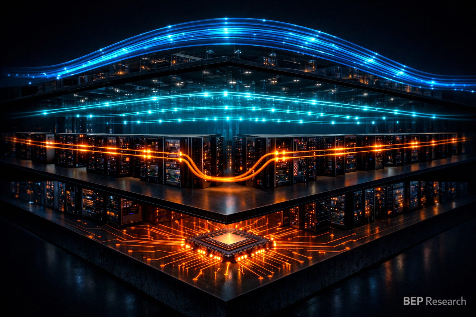
One company. Every connectivity layer from silicon to building:
Weaver → chip-to-memory, 10 inches. Memory Wars. FY28.
AECs → 0–7m, rack scale. $407M/quarter. De facto standard.
ALCs → 7–30m, row scale. Micro-LED. FY28. (“Credo wins both sides of this trade. AECs today. Active Light Cables tomorrow.”)
ZeroFlap → any length optical. Production ramp Q1 FY27.
Collectively: $10B+ addressable market. No other company covers the full spectrum.
Q4 guide isn’t a demand cliff — it’s mix. Still guiding to 200%+ full-year growth.
NVIDIA just put $4 billion behind the optical thesis — $2B each into Lumentum and Coherent, the same day Credo reported. The companies NVIDIA invested in sit above Credo in the stack.
Memory Wars has a new front. Weaver reveals the physical interconnect between memory and compute is its own bottleneck. I’ll have more on this at GTC.
$407 million. 202% YoY. And they say we’re early.
GTC is two weeks away. I’ll be there covering Jensen’s keynote, the optical and memory sessions, and the angles no one else is tracking. BEP Research is going paid soon — subscribe now to lock in free access and get a special founding member offer when we launch.
Subscribe to BEP Research →
About the Author
Ben Pouladian is a Los Angeles-based tech investor and entrepreneur focused on AI infrastructure, semiconductors, and the power systems enabling the next generation of compute. EE degree from UC San Diego. Chairman of the Leadership Board at Terasaki Institute for Biomedical Innovation. YPO member. Long-term NVIDIA investor since 2016.
Follow on Twitter/X: @benitoz | More at benpouladian.com
Disclosure: The author holds positions in NVDA, CRDO, LITE, and ALAB. This is not investment advice.


Leave a Reply