16 min read
Four data points converged this week that, individually, look like routine product news. Together, they’re the most significant validation of Apple’s AI infrastructure strategy since WWDC 2025.
Apple launched the M5 Pro and M5 Max MacBook Pro – the company’s first chiplet-based consumer silicon. Apple upgraded Private Cloud Compute to M5 chips, skipping M3 and M4 entirely. Ivan Fioravanti posted Qwen3.5-397B running at 38 tokens/second on an M3 Ultra via MLX. And Adrien Grondin posted Qwen 3.5 2B running on-device on iPhone 17 Pro via MLX.
Read those together. Apple now has a three-layer inference architecture – on-device, private cloud, and partner – running the same silicon DNA from phone to server rack. That’s not a product announcement. That’s an infrastructure moat.
In The Other Memory Wall, Part 1, I argued that NVIDIA owns the datacenter side of the memory wall, but Apple is building a moat on the other side – the edge.
The core thesis: Apple’s unified memory architecture eliminates the PCIe tax that cripples x86 machines running local LLM inference. While an RTX 4090’s 24GB VRAM forces aggressive quantization on anything above 13B parameters, a Mac Studio with 192GB unified memory runs 70B+ models without breaking a sweat. No PCIe bus to cross. No separate VRAM. No data copying between address spaces. MLX – Apple’s framework co-designed for unified memory – compounds the advantage by assuming zero-copy operations and unified memory allocation.
The Clawdbot/Moltbot phenomenon proved the thesis empirically. Silicon Valley developers weren’t buying Mac Minis because they’re Apple fans. They were buying them because the architecture matches the workload.
Part 1 ended with a claim: NVIDIA owns one side of the memory wall, Apple is building a moat on the other.
Today, that moat got three layers deep.
The M5 Pro and M5 Max aren’t iterative upgrades. They’re built on what Apple calls Fusion Architecture — the company’s first multi-die consumer silicon, combining two 3nm dies into a single SoC. The implications go beyond specs.
Apple’s design uses a shared 18-core CPU (6 “super cores” + 12 performance cores) across both Pro and Max variants. The M5 Pro pairs it with a 20-core GPU. The M5 Max doubles that to 40 GPU cores. Same CPU die, different GPU configuration. And critically: each GPU core now includes a Neural Accelerator, delivering up to 4x faster LLM prompt processing than the previous generation. This is the chiplet playbook that AMD pioneered with EPYC and that NVIDIA is executing with Blackwell’s multi-die design — but Apple is bringing it to consumer laptops with AI inference baked into the GPU itself.
Why this matters for inference: the M5 Ultra is now inevitable. Apple’s Ultra chips have always been two Max dies fused via UltraFusion interconnect. Two M5 Max dies give you an 80-core GPU and up to 256GB of unified memory — with the M5 Max already confirmed at 614GB/s bandwidth, the Ultra could approach 1.2TB/s across the fused die.
Let that sink in. 256GB unified memory in a workstation. A 400B+ parameter model at 4-bit quantization — or a 120B+ model at full FP16 precision — fitting entirely in a single machine’s memory pool, accessible at potentially over 1TB/s bandwidth across GPU, CPU, and Neural Engine simultaneously.
But the chiplet story has a deeper implication. By standardizing the CPU die across Pro and Max, Apple is building the same modular scaling strategy that dominates datacenter silicon. The same die that goes in your MacBook Pro can be tiled into a Mac Studio, a Mac Pro, and – crucially – a Private Cloud Compute server node. Same silicon. Same memory architecture. Same software stack.
That’s not a product family. That’s an inference platform.
Two recent posts from the MLX community turned architectural theory into observable reality.
Ivan Fioravanti (@ivanfioravanti) – the Milan-based developer who’s become the unofficial benchmark king for Apple Silicon inference – posted Qwen3.5-397B-A17B running via MLX on an M3 Ultra with 512GB. At 4-bit quantization, the model generates at 38 tokens/second at short context lengths, dropping to 24 tok/s at 128k context. A 397-billion-parameter MoE model with 17B active parameters, running locally, at conversational speed.
That’s not a toy demo. 38 tok/s on a model this capable is faster than what most cloud API endpoints deliver. And this is on an M3 Ultra – a chip that’s now two generations old.
On M5 Ultra, with its higher memory bandwidth and improved Neural Accelerators? Apple demonstrated 19-27% faster token generation on M5 versus M4, tracking linearly with the bandwidth improvement. Extrapolate across the M3-to-M5 gap, and that 38 tok/s likely pushes toward 45-50 tok/s at short context – well past GPT-4o API response times. Running locally. No cloud dependency. No subscription. No data leaving your machine.
Meanwhile, Adrien Grondin posted Qwen 3.5 2B at 6-bit quantization running on-device on iPhone 17 Pro via MLX. Not through Apple’s Foundation Models framework – through the open-source MLX ecosystem, running a third-party model on a phone. The post went viral — 1.8 million views — and Alibaba’s own account amplified it.
These two data points bracket the entire inference spectrum. A 2B model on your phone for instant, private, latency-free responses. A 397B model on your workstation for frontier-class reasoning. Both running on MLX. Both leveraging unified memory. The only difference is how many transistors and LPDDR packages sit between the user and the answer.
The software co-design thesis from Part 1 isn’t theoretical anymore. MLX on Apple Silicon isn’t just “fast.” It’s enabling workloads that the x86 + discrete GPU ecosystem physically cannot serve.
Apple upgraded Private Cloud Compute to M5 silicon. They skipped M3. They skipped M4. They went straight to M5.
That’s not a routine infrastructure refresh. That tells you three things.
First: Apple considers PCC strategically important enough to dedicate its latest silicon immediately. PCC isn’t a side project. It’s core infrastructure, getting the same priority as flagship consumer hardware.
Second: The M5’s chiplet architecture matters for servers. The same modular die strategy that enables Pro/Max/Ultra consumer chips enables dense, power-efficient server nodes. Apple can tile M5 dies for cloud inference with the same building blocks it uses for laptops – collapsing the engineering overhead of maintaining separate server silicon.
Third: The PCC Agent Worker appearing in iOS 26.4 signals that Apple’s on-device/cloud orchestration is becoming real-time and seamless. Your iPhone decides what runs locally and what gets routed to PCC based on model size, latency requirements, and computational complexity. The user never sees the boundary. And Apple is manufacturing these PCC servers domestically — in a Houston, Texas factory, part of its $600 billion U.S. infrastructure commitment. Analyst Ming-Chi Kuo reports that dedicated AI server chips (distinct from the M-series) begin mass production in late 2026, deploying in 2027. The M5 PCC rollout is the bridge.
This is the middle layer – the one most analysts are missing. Apple’s AI strategy isn’t just “on-device” versus “cloud.” It’s a private cloud that runs on the same unified memory architecture as your phone and laptop. The model weights, the memory access patterns, the MLX optimizations – they’re identical whether the inference happens on your M5 MacBook Pro or on an M5 PCC server node in Apple’s datacenter.
No other company has this. Google’s cloud runs on TPUs while your Pixel runs on Tensor chips – different architectures, different software stacks, different optimization targets. Microsoft’s cloud runs on NVIDIA GPUs while your Surface runs on Qualcomm – completely different worlds. Amazon’s cloud runs on Trainium while your Kindle runs on… nothing relevant.
Apple has one architecture, one framework, one memory model, from phone to cloud. That’s co-design at infrastructure scale.
The tech press narrative frames Apple’s use of Google Gemini as a concession – Apple couldn’t build frontier models, so they outsourced to Google. That reading is exactly wrong.
Gemini is Apple’s third inference layer – and it’s the layer Apple deliberately chose not to build. Not because they can’t, but because the economics and strategy don’t require it.
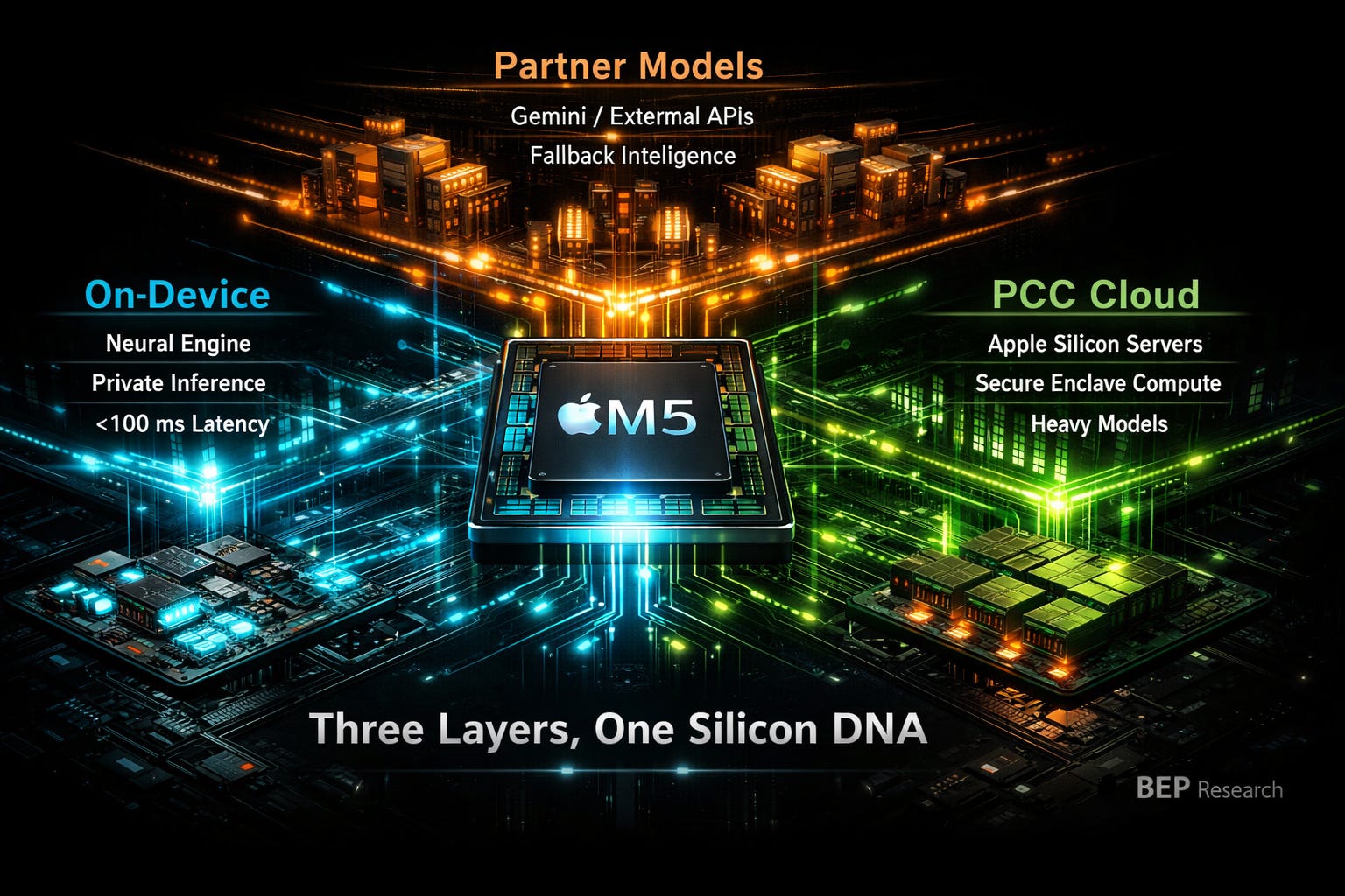
Think about what Apple’s three-layer architecture actually looks like:
Layer 1: On-Device. Small models (2B-7B) running on iPhone, iPad, Mac via MLX and Apple’s Foundation Models framework. Instant latency. Complete privacy. Handles the majority of daily AI interactions – autocomplete, summarization, image understanding, quick Q&A.
Layer 2: Private Cloud Compute. Medium-to-large models (30B-200B+) running on Apple’s M5-powered PCC servers. Sub-second latency. Apple’s privacy guarantees – your data is processed on Apple Silicon in secure enclaves, never stored, never accessible to Apple employees. Handles complex reasoning, long-form generation, multi-step tasks.
Layer 3: Partner (Gemini). Frontier-class models for the long tail of requests that require capabilities beyond what Apple’s own models or PCC can serve. The user explicitly opts in. Apple doesn’t send data to Google by default – the user chooses, per request, whether the task warrants a third-party model.
This is a division of labor, not a concession. Apple captures the vast majority of inference workloads – the ones that happen millions of times per second across a billion devices – on hardware it controls completely. Gemini handles the edge cases. Google gets API revenue. Apple gets to avoid the tens of billions in training compute investment that frontier model development requires.
The strategic insight: Apple doesn’t need to win the frontier model race. They need to win the inference deployment race. And with same-architecture silicon from phone to private cloud, they’re building a moat that model providers can’t cross.
Here’s what makes Apple’s position architecturally unique – and why it’s so difficult to replicate.
I walked through the competitor fragmentation in the PCC section above. But the deeper point isn’t just that rivals have split stacks — it’s that reunifying them is a decade-long project. Google would need to merge TPU and Tensor architectures. Microsoft would need to build its own silicon from client to cloud. NVIDIA would need to acquire a device platform. None of these are plausible on a competitive timeline.
Apple has one unified memory architecture spanning:
The A19 Pro in iPhone 17 Pro. The M5 in MacBook Pro, Mac Studio, Mac Pro. The M5 in Private Cloud Compute server nodes. All sharing the same LPDDR memory interface. All running MLX. All optimized for zero-copy, unified memory access patterns.
When Apple’s ML team optimizes a model for PCC deployment, those optimizations transfer directly to on-device inference. When an MLX contributor like Ivan Fioravanti benchmarks Qwen3.5 on an M3 Ultra, the performance characteristics predict what the same model will do on an M5 PCC node – because the memory architecture is identical.
This is co-design at a scale that goes beyond what I described in my original Co-Design Series about NVIDIA. NVIDIA co-designs hardware and software within the datacenter. Apple co-designs hardware, software, and deployment topology across the entire inference surface – from pocket to cloud.
There’s a dimension here that semiconductor analysts consistently undervalue because it doesn’t show up in spec sheets: privacy as infrastructure.
Apple’s business model is hardware margins. They sell you a $3,499 MacBook Pro and a $1,199 iPhone. They don’t need your data. They don’t need to train models on your conversations. They don’t need to serve you ads based on what you asked your AI assistant.
Google’s business model is data. Gemini is brilliant, but every interaction feeds the broader ecosystem. That’s not a criticism – it’s a structural reality that shapes architectural decisions.
Apple’s three-layer architecture turns this into a competitive advantage. Layer 1 data never leaves your device — Apple never sees it. Layer 2 data is processed in PCC’s hardware-isolated secure enclaves and immediately discarded — no logs, no model training, no employee access. Layer 3 is explicit opt-in — the user chooses when a request goes to Gemini.
Here’s the line that should be on every investor’s mind: your data shouldn’t train someone else’s model. Apple sells hardware, not data. That’s not just a marketing message – it’s an architectural commitment that shapes every silicon decision, every framework optimization, every deployment choice.
For enterprise buyers evaluating AI deployment – law firms, healthcare systems, financial institutions, government agencies – this isn’t a nice-to-have. It’s a procurement requirement. And Apple is the only major platform where the privacy guarantee is enforced by hardware architecture, not just policy.
For AI infrastructure investors, these four data points validate a thesis that requires repositioning how we think about the AI value chain.
Apple – The only company with vertically integrated inference silicon spanning consumer devices to private cloud. The M5 chiplet architecture enables cost-efficient scaling. PCC creates a recurring infrastructure moat that justifies premium hardware pricing. The privacy architecture is a structural advantage in enterprise AI adoption. This isn’t an NVIDIA competitor — it’s a parallel inference economy with a different business model and different winners.
NVIDIA – Still dominates training and datacenter batch inference. The Gemini partnership actually validates NVIDIA’s position: Apple’s Layer 3 runs on Google TPUs and NVIDIA GPUs in Google’s cloud. But NVIDIA has no answer for Layer 1 and Layer 2 – the on-device and private edge inference workloads that represent the next billion AI interactions. DGX Spark was a recognition of this gap, but LPDDR5X at 273GB/s can’t match Apple’s unified memory efficiency for single-stream inference.
Google – Benefits as a Layer 3 partner, collecting API revenue from Apple’s overflow traffic. But the partnership is asymmetric: Apple controls when and whether traffic reaches Gemini. Google is a supplier, not a platform, in Apple’s architecture. TPU investment remains critical for Google’s own products, but the Apple relationship is incremental revenue, not a strategic moat.
Qualcomm – The most exposed competitor. Snapdragon X Elite makes similar unified memory claims, but lacks the software co-design (MLX equivalent), the cloud layer (PCC equivalent), and the privacy architecture. Windows + generic ML frameworks can’t match Apple’s vertical integration. Qualcomm’s AI PC narrative becomes significantly harder to sell when Apple demonstrates frontier-class models running on two-generation-old hardware.
Memory vendors (SK Hynix, Samsung, Micron) – Apple’s architecture is LPDDR-based, not HBM. As Apple scales PCC and sells more high-memory-configuration Macs, LPDDR demand from AI workloads increases – potentially providing a tailwind for LPDDR pricing that partially offsets the DRAM/SRAM cost convergence I covered in Raja Was Right. But Apple’s efficiency means they need less total memory bandwidth per inference workload than HBM-based alternatives, which limits the volume story.
M5 Ultra announcement timing. Apple typically reveals Ultra chips 3-6 months after Max. If M5 Ultra ships with 256GB unified memory and bandwidth scaling from the M5 Max’s confirmed 614GB/s, it validates the “desktop supercomputer for inference” thesis at a price point enterprises will actually pay.
PCC capacity buildout. Apple hasn’t disclosed how many M5 PCC nodes they’re deploying. The scale of this investment – and whether Apple starts offering PCC as an enterprise service – determines whether Layer 2 becomes a real business or remains a consumer feature.
MLX ecosystem momentum. Ivan Fioravanti’s Qwen3.5-397B benchmarks and Adrien Grondin’s iPhone demo are community-driven. Watch for Apple’s own model releases at WWDC 2026. If Apple ships 30B+ Foundation Models optimized for M5’s Neural Accelerators, the on-device layer gets significantly more capable.
Gemini integration depth. How much traffic does Apple actually route to Layer 3? If on-device and PCC handle 95%+ of requests, Gemini becomes a safety net rather than a dependency – strengthening Apple’s position further.
Enterprise adoption signals. Law firms, healthcare, finance – any industry with data sovereignty requirements is a natural Apple PCC customer. Watch for enterprise-specific PCC announcements, especially around HIPAA and SOC 2 compliance.
GTC 2026 (March 16). I’ll be on-site. NVIDIA’s response to Apple’s edge AI positioning will be worth watching – particularly any announcements around inference-optimized silicon for non-datacenter workloads.
BEP Research is going paid on March 9. Annual subscriptions are $400/year, but through March 9 you can lock in the early-bird rate of $350/year. Once the paywall goes up, the discount goes away. If you’ve been reading for free and finding value, now is the time.
GTC 2026 starts March 16. I’ll be there in person. On-site analysis of NVIDIA’s architecture announcements, networking roadmaps, and co-packaged optics developments will be a cornerstone of paid subscriber coverage.
Subscribe to BEP Research →
Most AI infrastructure analysis focuses on the datacenter. Training clusters. HBM bandwidth. NVLink topologies. That analysis is correct – and I’ve spent months building the case for why NVIDIA’s co-design advantage is durable in that arena.
But these four data points prove that inference has a second front. Apple isn’t competing with NVIDIA for datacenter dominance. They’re building a parallel inference economy – one where the same silicon architecture spans from phone to private cloud, where software co-design means a 397B model runs at nearly 40 tokens/second on a desktop, and where privacy is enforced by hardware, not policy.
NVIDIA owns one side of the memory wall. Apple is building a moat on the other. And that moat is three layers deep.
Related BEP Research
About the Author
Ben Pouladian is a Los Angeles-based tech investor and entrepreneur focused on AI infrastructure, semiconductors, and the power systems enabling the next generation of compute. He was co-founder of Deco Lighting (2005-2019), where he helped build one of the leading commercial LED lighting manufacturers in North America. Ben holds an electrical engineering degree from UC San Diego, where he worked in Professor Fainman’s ultrafast nanoscale optics lab on silicon photonics and micro-ring resonators, and interned at Cymer, the company that manufactures the EUV light sources for ASML’s lithography systems.
He currently serves as Chairman of the Leadership Board at Terasaki Institute for Biomedical Innovation and is a YPO member. His investment research focuses on AI datacenter infrastructure, GPU computing, and the semiconductor supply chain. Long-term NVIDIA investor since 2016.
Follow on Twitter/X: @benitoz | More at benpouladian.com
Disclosure: The author holds positions in NVIDIA, Apple, and related semiconductor investments. The author may initiate positions in companies mentioned in this article. This is investment research, not advice. Do your own work.


Leave a Reply